How RAM Works
If you would like to test out this circuit for yourself, try this website for simulating it.
To store one bit of data we need two NAND logic gates. A NAND logic gate is an and, and a not. If you are not familiar with logic gates I will briefly explain.
Logic Gates
Logic gates are pieces of hardware that perform logical operations such as "AND", "OR", "Exclusive OR", and "NOT". They deal with digital logic, 1's and 0's or high and low. For example an AND gate with two inputs requires both inputs to be high for the output to be high, any other input will have a low output. An OR gate, either or both can be high to have a high output, an Exclusive or either input being high (but not both) will result in a high output, and a not just flips the output. This circuit deals with NANDS (AND + NOT) so I will give you the truth tables for that logic gate showing every possible combination.
NAND
Input A | Input B | Output
0 | 0 | 1
0 | 1 | 1
1 | 0 | 1
1 | 1 | 0
Latch Circuit
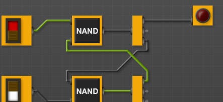
A latch circuit uses two NAND logic gates and holds one bit of information. When you think about how many bits of RAM your phone or computer or any of your electronics has, it is really amazing. So to store this bit of data with two NAND gates, they have to be connected the right way. The output of each NAND will go to one of the inputs of the other NAND. One of the outputs, will also be the output where the bit is stored. The remaining two inputs (one on each NAND gate) control this. One acts as a reset switch, the other as a set switch. When the reset switch is flipped, the output will 0 no matter how many more times you flip the reset switch. When the set switch is flipped, the output will stay 1, no matter how many times the set switch is flipped. This allows you to set and reset whether the bit is high or low and keep it set to that position until you want to reset it. Which input is set vs reset depends on which output you are measuring.
Explaining circuits with text is never easy, so here is a picture of it using this website.
The top NAND is set and the bottom NAND is reset.
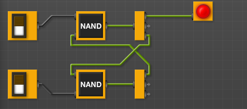
So lets test this circuit.
First, lets turn both switches off.
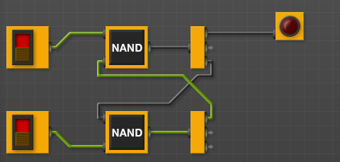
Now lets hit set once to set the bit as high.
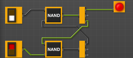
Note that the light turned on. Try flipping set again.
Flip the set switch as many times as you like, it will stay on.
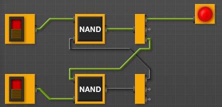
Now we will flip reset to turn it off. Keep flipping reset as many times as you want, it will stay off.
There are 8,000,000,000 bits in one gigabyte. That is a lot of latches. Really gives you an appreciation for the massive amounts of RAM we can fit into such tiny chips.
You will notice that the site I linked you to to simulate this has a category called flip flops, one of which is the circuit we just built with NANDS.
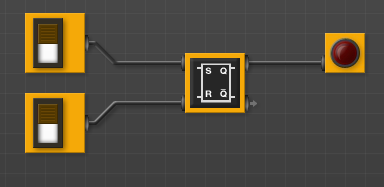
If you want to try and build your own logic gate circuit with memory for fun, now you can. If you make something cool be sure to share it.
I made something real quick to show how multiple latches can be used to store a value.
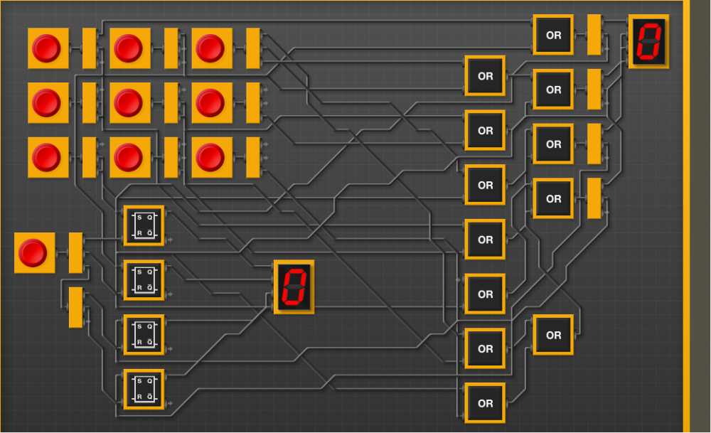
Now lets press the 7 button.
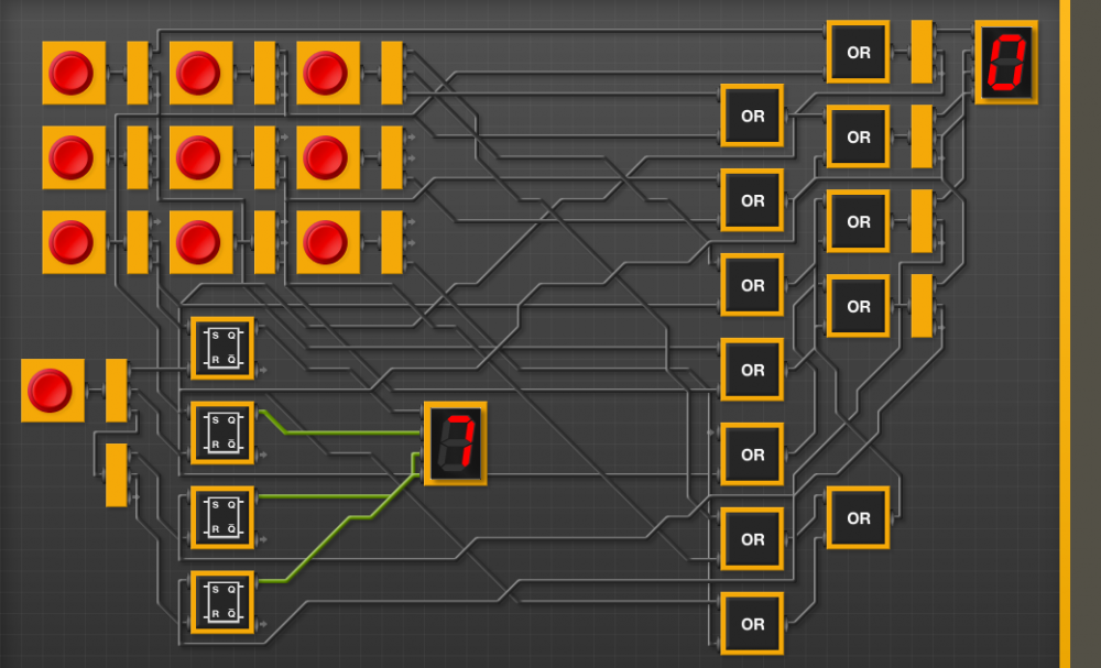
You can see that on the screen to the right, after a button is pressed it forgets what button was hit, while the screen on the bottom remembers what button was pressed.
Try for yourself! (The lone button resets it so you can enter a new number)
If you make this you will notice that which pin is set to high on the LCD, means different things. 1, 2, 4, and 8. These values are added then the sum is displayed on the LCD. Because of this each bit we store with the latch means something different. This is known as the memory's address. This is how RAM works everywhere. In micro controllers such as the PIC, editing the values of a register can do different things, such as change the pin mode or other settings so it is important to know what that registry does before changing any values.